| Restocking Fee | No |
|---|---|
| Return shipping will be paid by | Buyer |
| All returns accepted | Returns Accepted |
| Item must be returned within | 30 Days |
| Refund will be given as | Money Back |
| Compatible Brand | Universal |
| Type | Echo Canceller |
| MPN | TECO32642 |
| Brand | Lucent |
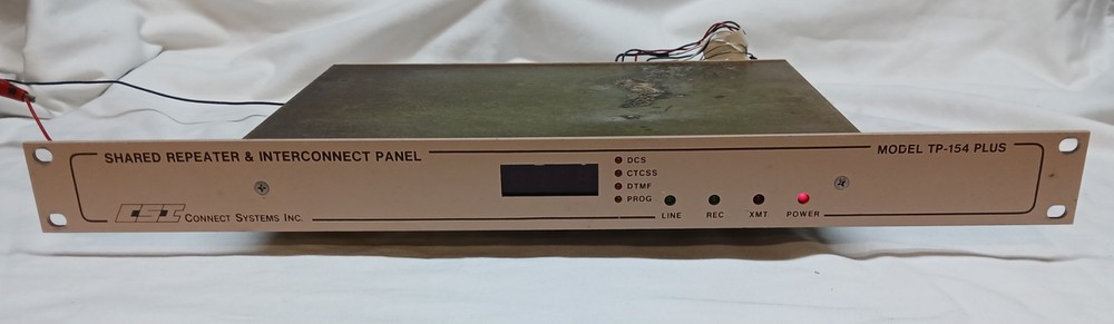
Check the listing for details. Lucent TECO32642 Dual-convergence Voiceband Echo Canceller 32 Channel. Condition: New. Listed at 39.95 USD. Old Inventory of Lucent TECO32642 Dual-convergence Voiceband Echo Canceller 32 ChannelFeaturesApplicationsDual-convergence voiceband echo canceller (EC). 32 independent and individually controlled echo canceller channels. Stable performance across virtually all network hybrid conditions. Multiple-channel processing modes: Echo cancelling ON/OFF. µ-law to A-law and A-law to µ-law conversion. 64-clear. Tail-end delay to 64 ms. Flexible integrated nonlinear processor. Automatic echo path change detection. PCM interface supporting µ-law, A-law, and linear formats. Two independent tone disablers. Two-band tone detection. Multiple-configuration options for tone disabling: 2100 Hz. 2100 Hz with phase reversal only. 2010 VPA. Dual band. None. Integrated data storage in on-chip SRAM. Integrated PLL for high-speed operations. High-speed microprocessor interface configurable to operate with most commercial microprocessors. Built-in self-test and boundary scan. IEEE *1149.1 boundary scan (JTAG). ITU-T G.165, G.168 compliance. Highly provisionable and highly observable. Selectable 5.0 V tolerant inputs. 85 °C temperature range. Typical power dissipation: 700 mW--900 mW. 160-pin, plastic, metric quad flat pack with heat spreader (MQFPH) package.Digital terrestrial communication networks Digital wireless communications networks Digital personal communication networks Voiceband telephony Voice calls Low-speed modem calls Voice over Internet Packetized voice (e.g., frame relay, ATM) Centralized applications Local exchange (LEC) office Interexchange (IEC) office Mobile telephone switching office (MTSO) Base-station controllers Packetized voice equipmentDescriptionThe TECO3264 32-channel echo canceller (EC) device 3.3 V, CMOS, very large-scale integration (VLSI) component offering 32 independent channels of echo cancellation. Packaged a 160-pin, plastic, metric quad flat pack with heat speader (MQFPH) and handling ms of tail-end delay, this device combines high performance, high channel density, low power dissipation, high flexibility, excellent maintenance capability, and low cost into a single package. The TECO3264 32-channel echo canceller provides echo cancellation for both T1 and E1 systems. The device operates from a single 3.3 V supply and requires only an external 8.192 MHz clock and 8 kHz frame sync. Built-in self-test logic affords easy device verification while integrated boundary-scan capability reduces board verification time and cost. A high-speed microprocessor interface and full user provisionability on device pins provide maximum flexibility.* IEEE is a registered trademark of The Institute of Electrical and Electronics Engineers, Inc.Features................................................................................................................................................................... 1 Overall Device.............................................................................................................................................. 1 Applications.............................................................................................................................................................. 1 Description................................................................................................................................................................ 1 Block Diagram.......................................................................................................................................................... 8 Pin Information......................................................................................................................................................... 9 Pin Assignment............................................................................................................................................ 9 Pin Descriptions......................................................................................................................................... 10 Functional Description............................................................................................................................................ 13 X(PCM/Linear) Highway Control (XPCM).................................................................................................. 13 Y(PCM/Linear) Highway Control (YPCM).................................................................................................. 13 E(PCM/Linear) Highway Control (EPCM).................................................................................................. 13 Convolution/Update Processor (CUP)........................................................................................................ 13 Nonlinear Processor (NLP)........................................................................................................................ 13 Tone Disablers TD2)........................................................................................................................ 13 Microprocessor Interface and Control (MPIC)............................................................................................ 13 External Control Connection................................................................................................................................... 14 Microprocessor Interface and Control (MPIC)............................................................................................ 14 Channel Status and Control....................................................................................................................... 19 PCM Input/Output (I/O) Timing and Register Control................................................................................. 20 H-Register Channel Status......................................................................................................................... 30 Parameters............................................................................................................................................................. 34 Parameter Overview................................................................................................................................... 34 Per-Channel Control Parameters............................................................................................................... 34 Mask Bits.................................................................................................................................................... 35 Echo Canceller (EC) Parameters............................................................................................................... 36 PCM Transmission Parameters................................................................................................................. 37 Tone Disabler Parameters......................................................................................................................... 40 Nonlinear Processor Parameters............................................................................................................... 41 Control Parameters.................................................................................................................................... 42 Test and Diagnostic Parameters................................................................................................................ 43 Parameter Map....................................................................................................................................................... 45 Register Architecture.............................................................................................................................................. 48 Register Scopes......................................................................................................................................... 48 Registers, Functions, Symbols--Information Presentations...................................................................... 49 Recommended Register Values................................................................................................................. 50 Notation and Format: Bits per Parameter and Bits in Registers................................................................. 50 Recommended Register Values for DS1 (µ-Law)...................................................................................... 51 Recommended Register Values for E1 (A-Law)........................................................................................ 52 Function Name to Symbol and Register Address Index............................................................................. 53 Symbol to Register Address and Function Name Index............................................................................. 59 Page 0 Read/Write Registers 000--07FE.................................................................................................. 65 Page 1 Read-Only Registers 100--10E................................................................................................... 114 Absolute Maximum Ratings.................................................................................................................................. 119 Recommended Operating Conditions.................................................................................................................. 119 Electrical Characteristics...................................................................................................................................... 119 Input and High-Impedance Leakage Current........................................................................................... 119 Clock Input Specifications........................................................................................................................ 120 Other Input Specifications........................................................................................................................ 121 Output Signal Specification...................................................................................................................... 123Physical Characteristics........................................................................................................................................124 Outline 160-Pin MQFPH........................................................................................................................................125 Ordering Information.............................................................................................................................................126 DS99-241PDH Replaces DS98-409TIC to Incorporate the Following Updates....................................................126
You may also like